Disclaimer
This information HAS errors and is made available WITHOUT ANY WARRANTY OF ANY KIND and without even the implied warranty of MERCHANTABILITY or FITNESS FOR A PARTICULAR PURPOSE. It is not permissible to be read by anyone who has ever met a lawyer or attorney. Use is confined to Engineers with more than 370 course hours of engineering.
If you see an error contact:
+1(785) 841 3089
inform@xtronics.com
Pcbnew
Related kicad pages
-
EE CAD Terminology
-
kicad Navigator - the kicad project Manager
-
eeschema - the schematic editor
-
cvpcb - the component to module (AKA foot-print) editor
- pcbnew - the PCB layout program
-
Gerbview - the Gerber file viewer and production
notes
-
Bitmap2Component Converts bitmap images
to filled polygons
-
wings3d - 3d view - good way to waste a lot of
time..
Layers
Probably the best place to start is to look at the layers used in PcbNew. Find the Layers Manager toolbar.
Some of the Nomenclature needs clarification:
- Copper Layers - This is what other packages might call Tracks - does not include pads and via pads
- Front - component 15
- Back - Solder - 1
- Inner_Lx Are inner connecting copper layers where 'x' refers to which layer. Layers between 2 - 14 are inner layers.
- Tech Layers
- Adhes_Back - 16 - is the Adhesive screen on the 'solder side'. Normally there would be no adhesive on this side unless the part
is flipped to the opposite side.
- Adhes_Front - 17 - is the Adhesive screen on the normal part side.
- SoldP_Back - 18 - Solder paste - (not normally used on back) where it is applied on pads with this layer turned off on Module
pad or where drawn on PCB
- SoldP_Font - 19 - Solder paste - (not normally used on back) where it is applied on pads with this layer turned off on Module
pad or where drawn on PCB
- SilkS_Back - 20 - Silk Screen - used on back for notation mostly - and through-hole parts
- SilkS_Front - 21 - Silk Screen - same layer as reference.
- Mask_Back - 22 - Solder mask - used automatically with thru-hole parts - if mask is turned off on module pad - this is where
solder mask is NOT
- Mask_Front - 23 - used automatically with both thru-hole and SM parts - if mask is turned off on module pad - this is where
solder mask is NOT
- Drawings - 24 - Dimensions etc
- Comments - 25 -
- ECO1 - 26
- ECO2 - 27
- Board edge - 28
- Plating (coming soon)
- HoleFill (coming soon)
- KeepOut for component, plane, trace and via keepouts and keepins. (coming soon)
- ViaPlug (coming soon)
- Contacts (coming soon)
- PeelMask (coming soon)
- Finsh (coming soon)
- Courtyard for component courtyards (coming soon)
- Component for component outlines for assembly drawings (coming soon)
- Coating (coming soon)
- Probe (coming soon)
- Fixture (coming soon)
Displaying layers
Pcbnew can display technical layers (like solder mask) but only in "high contrast mode"
- Select "high contrast display mode", this is the artist pallet on lower left toolbar.
- Select the technical layer you want to see.
Pads (and all items) that are on the selected layer are shown using this layer color Others are displayed in dark gray color.
Of course, in normal display mode, these layers are not displayed.
Board design Steps
Setting up DRC(Design Rules Check)
Importing Netlist and associated dialogs
- Make sure the librarys and paths are set correctly
- Basic Reading of the netlist
- click on the netlist button and look at the dialog
- select netlist file
- Bad Tracks Deletion needs to be set to "Delete"
- Exchange Module
- Change allows updating modules
- Extra Footprints
- Keep allows keeping of hardware holes etc..
- Timestamp
- This causes the modules to be identified by their timestamp rather than the reference number. uesed when there are changes to the
Reference numbers - back up first before trying this.
- Rebuild Board Connectivity
- Reconnects the board parts based on _______ ?(net list? any exceptions? ) - need a precise explanation of what happens
here.
- Footprint test
- Returns no modules if non found. What else?
Placement
Routing
Hand Routing
- edit/Cleanup_tracks_and_via
- Be aware that those extra via's used to put in test points or stitch ground planes can be deleted here.
- The connect to pads option is very useful if you have changed to smaller resistor or capacitor cases.
Auto Routing
Freerouter
Most people are using Freerouter.
- Paths and zones placed before routing are left alone.
Built-in Auto Router
Creating Copper Ground planes - Zones
- Select Add Zones icon
- Trace the limit of the zone
- Place the cursor on a pad belonging to the net you want for the plane, (GND or any other)
- Click right on the zone and select fill zone
- Also see Connecting different net planes with a
Pavilion AKA Net-Tie
Vias
Alternate Via Drill
From the Tracks and Vias Sizes dialog box:
- This feature is used when some vias must have a specific drill size (which differs from the default drill size). You can adjust the
"Alternate Via Drill" to a correct value, and for some vias you can select this alternate value (by the pop-up menu) This job is more
easy if you have chosen a bigger (or smaller) via diameter for theses vias, because the pop-up menu has a command to export the current
via drill to all vias which have the same diameter (put the mouse cursor on such a via, and by the pop-up menu (edit via option) select
the alternate via drill for this via, and export the via drill to other identical vias (command edit via/export via drill to other id
vias)
Working with 4 layer boards
Setting up power layers
Setting up mixed layers
Panelize PCB
There are times when you want to put several copies on one pannel.
- Open PCBnew and display your board.
- Use select tool (arrow icon top of right hand icon bar) left click and draw a box around your board release mouse button
- move highlighted block OFF the drawing page somewhere this just gets it out of the way. You will get a move block requestor, make
sure all
options are ticked and click OK. Your board layout will then move.
- File menu > Append Board, then select the .brd file of your PCB then open.
A copy of your PCB will appear in the centre of the drawing page (that's why we moved the first copy)
- Use the block move method again to position your board where you want it,
then move the first copy back onto the board.
- Of course you can repeat this as many times as you want.
This method works if you want to place several different boards onto one drawing.
Another method if you want a copy of the same board, is to block select your board in the same way, then move it to the position you
want, but instead of left click, right click and you will get a context menu. select copy block, and your board will be copied to the new
location.
CAM Plot, Drill
- Do checks
- Set Pads Mask Clearance
- What exactly does "Solder mask ratio clearance mean?
- Hole count
- The number of holes in the PCB is found in the -drl.rpt file. They are listed by number and size.
Fiducial Marks
No one has ever asks for fiducials - and they spend time removing them and putting in their own. But if you insist: Global and/or
panel fiducials should ideally be located at three points of the grid. Locate a lower left fiducial at the 0,0 datum point and two
fiducials located in positive X and Y directions. These three marks help for correcting of non-linear distortions (scaling, stretch and
twist).
Global fiducials should be located on all PCB layers that contain components to be mounted with automated equipment. Using other
circuit objects (via-holes, etc.) ends up being a compromise.
Module Position File
Modedit
This is to create the modules AKA footprints. Once again, remember to always make a copy of a supplied footprint and save it in
your personal library directory in your own personal xxx.mod file
- A Pad with pin number 0 is not connected to any net - for structural use.
Module fields Reference and Value
- The field that has the module name becomes the reference designator (R1 for a resistor). The field that contains:
VAL**
reflects the Part name that pointed to the module.
Insert attibutes
Under module_editor/module_properties/attributes
- Normal is the standard attribute.
- Normal+Insert indicates that the module must appear in the automatic insertion file (for automatic
insertion machines) This attribute is most useful for surface mount components (SMDs).
- Virtual indicates that a component is directly formed by the circuit board. Examples would be edge
connectors or inductors created by a particular track shape (as sometimes seen in microwave modules).
- What is the difference between Normal and virtual - Virtual is for an edge card connector - but what is different?
Hole Types
- Standard - through hole pad
- SMD Surface mount (no hole) Hole has an electrical connection (used for through hole devices and/or Ground points)
- Connector - perhaps for an edge card connector??
Library Generation Considerations
Do not trust what is in the supplied library.
Checklist
Part Placement
- SMD component orientation consistent
- Clearance for IC extraction tools, heatsinks etc.
- Polarization of components checked
- Are components on grid ?
- Check the orientation of all connectors - is Pin #1 where you expect it?
- <inimum component body spacing
- Bypass capacitors located close to IC power pins
- Series terminators are located near the source
- I/O drivers near where their signals leave the board
- PCB has ground turrets, power rail test points, and test points for important signals, all labeled
- EMI and RFI filtering as close as possible to exit and entry points in shielded areas
- Potentiometers should increase controlled quantity clockwise
- Mounting holes electrically isolated or not?
- Mounting hole clearance for hardware
- SMD pad shapes checked
- Tooling holes for automated assembly
- Extra clearance for socketed ICs
- Pin one pad indicators
Routing
- Digital and analog signal commons joined at only one point - net tie - ground
Pavilion
- Check for traces running under noisy or sensitive components
- No vias under metal-film resistors and similar poorly insulated parts
- Traces spaced to max where possible
- Check for dead-end traces, unless used on purpose
- Ensure schematic software did / did not separate Vcc from Vdd, Vss from GND as needed (Not a problem if you don't use invisible
connections - it really doesn't save time in the long run )
- Multiple vias for high current and/or low impedance traces - check the current ratings of your via size
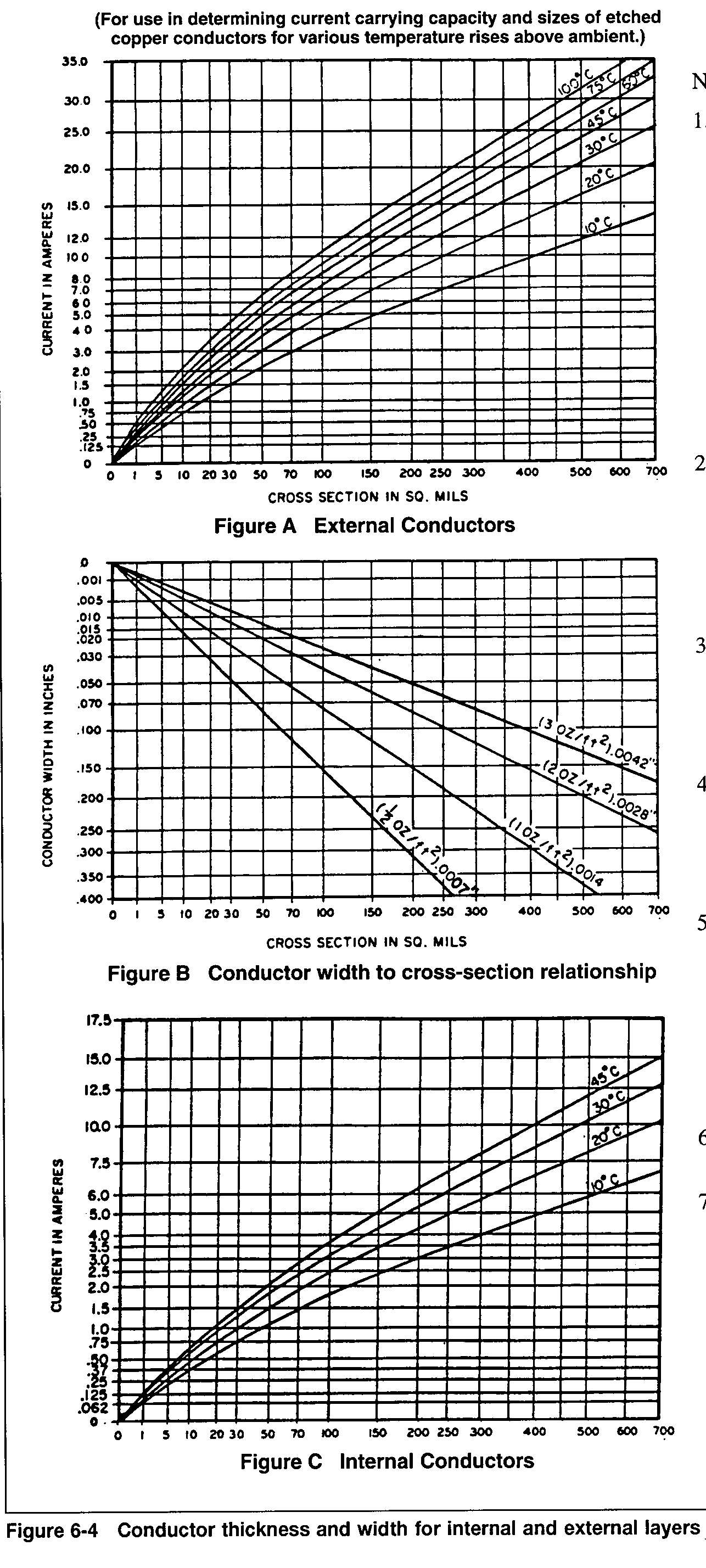
Current rating of Traces, viass
-
- Component and trace keepout areas observed
- Ground planes where possible
Dimensions
- Hole diameter on drawing are finished sizes, after plating.
- Finished hole sizes are >= 0.25mm larger than lead
- Silkscreen legend text weight, spacing
- Pads >=0.37mm larger than finished hole sizes
- Components spacing from edge of PCB
- Traces to board edge spacing
- Consider Drill size tolerance
- Soldermask clearance and tolerance - often board houses want zero clearance.
- High voltage traces need extra spacing
Text on Silk Screen and other Layers
- Allign legend text tp read from one or two orientations
- Logo in silkscreen legend
- Copyright notice
- PCB part number and version
- Do parts cover Legend
- Label all layers - Mirror text on back
- Pin one indicators
- High pin count parts can have corner pins numbered for ease of location
- Silk screen tick marks for every 5th or 10th pin on high pin count Parts
Tricks
Creating IPC compliant modules
To create foot prints that comply with ipc specs get
LP Calculator or
Lp_calculator_V2009 http://www.oldversion.com/PCB-Matrix-LP-Calculator.html(these run
under wine on linux).. There are three versions of the modules one can create for surface-mount work - General purpose - high reliability
and very-high density. (There are settings to get these numbers out of LP-calculator).
- A = Most - reliable - but bigger
- B = Nominal - mid sized
- C = Least - very small
One important detail: these case sizes originate in metric - the imperial notation is approximate. There are two ways that cap
footprints are specified - and it can generate confusion - metric and imperial - thus 0201 (02x01mils) = 0603 in metric (remind me to
once again curse the creeps that stopped metrication back in the '60s). Kicad's naming should be based on the modern metric codes. Thus a
0603 becomes 1608M and there should be three versions of the decal:
- 1608MM - most sized
- 1608MN - Nominal sized
- 1608ML - least sized
Going on step further we could have
- 1608MN02 be a metric 1608 Nominal sized land with 0.2mm thick so it can match something in the 3D renderer AND there is a
difference in the optimal land size depending on the height of the chip. This is also why we have C1608M and R1608M for chip-capacitors
and chip-resistors respectively. ( If the footprints are well optimized, there will be slight differences in height between resistors
and caps. )
I could also see having three libraries - as the SNM7351A SNL7351B SMN7351C.
Complete list of
SMT_Case_Size_Codes
- pcb-fpw is sort of an opensource version of LP_calculator. Download link
[1].
All of it is for supporting IPC-7351. pcb-fpw was written to support the competing opensource 'pcb' package - might work to have a
script to translate the modules?
pcb-fpw is open source, so it would be possible to modify add it to the kicad suite .. seems to be written in java-bloat.
Now there is
Madparts - not yet a nice package.
The separate names for a cap and resistor 0805 package seems silly unless we are using polarized caps. In which case we could have
- P1608MN02
And a diode in such a case
- D1608MN02
The M,N,and L are for most, Nominal and least -- describes most compromises folks would run into..
The modules should have a minimal silk screen and a part outline on the drawing level.
Custom case numbers that should probably be organized via part vendor.
Creating Module with Custom Solder-Paste

Very uglyNormally, the solder paste area is based on the pad area slightly reduced to keep paste off of non
pad areas. ( See Preferences/Dimensions/Pads_Mask_Clearance /Solder_Paste_Clearance in Pcbnew.) But for parts with larger pads that
provide heat-sinking, the amount of solder often needs to be reduced to keep the solder from balling up and causing the part to float to
high - or keeping mask out from under packages.
In the Module Editor go to Edit Pad which brings up the Pad Properties dialog. On the bottom left under Technical
Layers uncheck the SoldP_Front check-box which turns off the generation of solder-paste for this pad. Next, Using the Line, Circle,
or Arc tool - draw where you want solder-paste on this pad on the SoldP_Front layer. Sometimes it is better to use the next trick to
reduce the size thus reducing the height of solder due to surface tension.
It is probably the case that just a masking of the solder paste layer is all that is needed - reducing the contact area is only for
extreme floating problems - if the solder paste is reduced it is likely not a problem.
Preventing floating on heatsinking pads of SM packages
See bold note above
MLF/QFN devices, which have a thermal pad on the middle of the bottom. There are two considerations here.
- There is the heatsinking requirement
- A poor copper design wrong the chip will float on a central blob of solder, resulting in unreliable soldering of the pins.
For the thermal pad footprint for a 32 pin device arrange 8 square pads around a central via, and place solder resist over the via
Tented Via with the outer edge
of all the pads matching the pad on the bottom of the chip. The breaks in the pad to pad area limit the height of the solder ball due to
surface tension so the chip sits lower and closer to the board.
Number all the (thermal) pads as "33", so there is only one extra pin in eeschema. Connect together the pads and the via with a grid
of thick tracks. The use of a tented via in this way means that the via will be solidly connected to the heat-sinking copper zone on the
reverse side, whilst the tenting prevents solder wicking through the via. One could also put a via for all 9 locations bringing more heat
to the opposite side of the PCB.

MLF - Center area is about 3.1 x 3.1mm
Another way to accomplish this is put a large square pad under the MLF and then turn off both the solder-mask and solder paste output
in Pad Properties dialog and manually create the mask and paste in 9 zones.
similar advice
here
Via in pad
Pad Shapes
The last thing you want is a full 100% paste mask on the pad when it's under the component body of a low profile component. The
ability to mask the solder-paste is on the wishlist (2013).
For other parts a rounded-rectangle-pad-shape is superior to a rectangle-pad-shape because the aperture openings in the paste mask
stencil have to be rounded corners anyway - and the rounded corners or oval shape helps the surface tension keep the part aliened -
something that is much harder on no-lead parts.
Some people are claiming that rounded Rectangle Pad Shape are better than Oval (AKA oblong). This is not always the case - but does
help sell high end CAD systems. That being said, rounded rectangular pad shapes are the IPC preference for all Lands (except BGA, CGA and
LGA) including the chip parts like resistors and caps. There is
Importing DXF - DWG
Current rating rule of thumb - trace width - via size
- 100mils of 2oz copper will approximately carry 10A with some 20deg C temperature rise.
- Finished diameter of the via hole should be at least as large as the trace-width/3!
Other
- CAD design rule checking must be turned on
- High frequency circuitry precautions observed
- ReadMe for PCB house see
Gerbview#What_to_send_the_PCB_house checklist
- Thermal reliefs for internal power layers
- Solder paste mask spacing
- Blind and buried vias on multilayer PCB
- PCB layout panelization
Email