Disclaimer
This information HAS errors and is made available WITHOUT ANY WARRANTY OF ANY KIND and without even the implied warranty of MERCHANTABILITY or FITNESS FOR A PARTICULAR PURPOSE. It is not permissible to be read by anyone who has ever met a lawyer or attorney. Use is confined to Engineers with more than 370 course hours of engineering.
If you see an error contact:
+1(785) 841 3089
inform@xtronics.com
555 Delta-Sigma Modulator
Introduction
Inspired by the
555 Contest to come up with a novel use for the 555 timer, I crafted a
Delta-Sigma Modulator circuit that can be used as the basis for an audio amplifier, servo amplifier, A/D circuit, or most anywhere you
need an analog signal converted into a digital pulse stream. This circuit is original, at least to me. It seems like someone should have
done this already, but I was unable to find anything similar online. There are lots of 555 based class-D amplifiers, but all the ones I
found were using the control input and trying to PWM, rather than implement delta-sigma modulation. If you know of anything similar out
there, please let me know via e-mail (charles at steinkuehler dot net).
Videos with operating waveforms of the
basic circuit and
improved circuit are available on youtube.

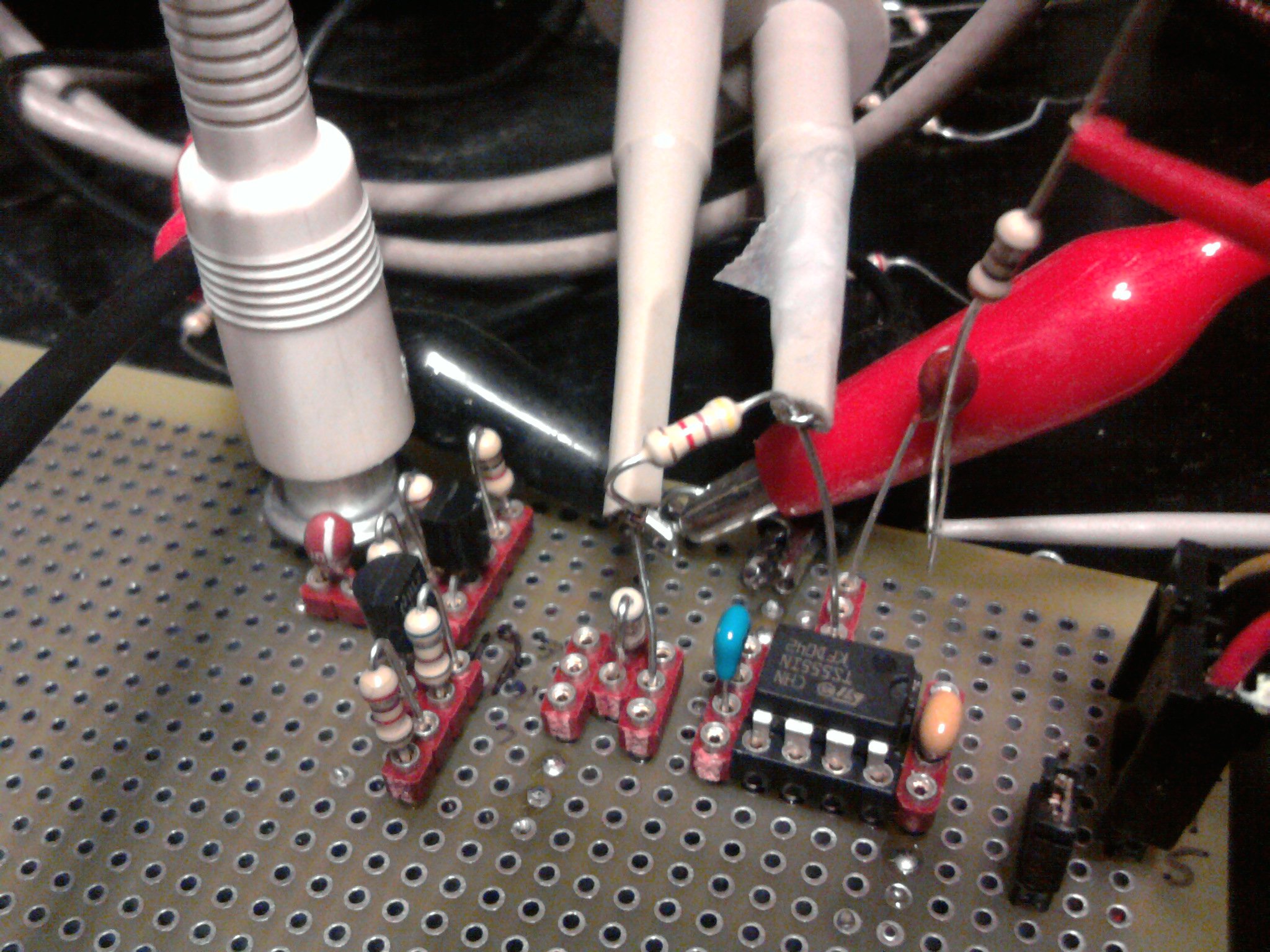
Fully functional 555 based
delta-sigma modulator
Background
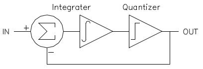
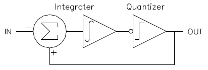
A delta-simga modulator is formed by quantizing the integral of the input signal minus the output.

With a simple transform (inverting the quantizer and changing the signs on the adder inputs), the above circuit turns into something
we can build with a 555.
The 555 delta-sigma modulator begins with a basic 555 astable circuit using just two external components: a resistor and capacitor to
set the timing.
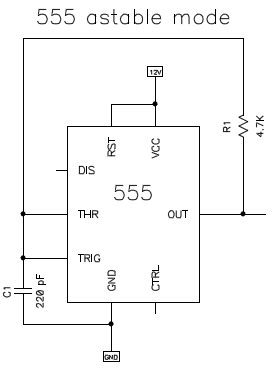
In the astable 555 circuit above, we already have two of the key delta-sigma components implemented. The resistor and capacitor from
an integrator with positive feedback from the output, and the 555s internal comparators functions as an inverting quantizer. Essentially,
you can think of the astable 555 timer circuit above as a delta-sigma modulator with a constant zero input, which yields a 50% duty cycle
output.
Basic Working Circuit
To provide for a signal input, we need a way to add the input term to the RC integrator network of the 555. Assuming a voltage input,
that means we need to connect a voltage to current converter between the input signal and the integrating capacitor, as shown in the
following schematic. Q12 forms a constant 1 mA current source, while Q11 is biased to sink 0 to 2 mA. This yields a net +/- 1mA
signal-based current being fed into the integrating capacitor C1, where it gets summed with the feedback from the output.
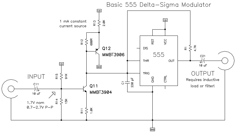
At this point, the circuit is a completely functioning delta-sigma modulator. The output can be filtered and used to efficiently drive
a load (class-D amplifier). You can also feed the pulse train into additional logic (ie: a micro-controller timer input) and create a
sigma-delta A/D converter.
Example waveforms of the operating circuit can be found
on youtube.
Improved Circuit
As an improvement, while the input voltage to current converter and the timing capacitor form a true integrator, the RC integrator for
the output feedback is less than ideal. The farther the output gets from 50% modulation, the more error is introduced by the RC feedback
circuit not functioning as a true integrator. Adding an additional voltage to current converter, or implementing current-source feedback
substantially improves the performance, particularly as the output level increases. Following is the basic delta-sigma modulator modified
to include constant-current feedback from the output. Also shown is the output filter used for performance testing.
Example waveforms of the improved circuit can be found on youtube.
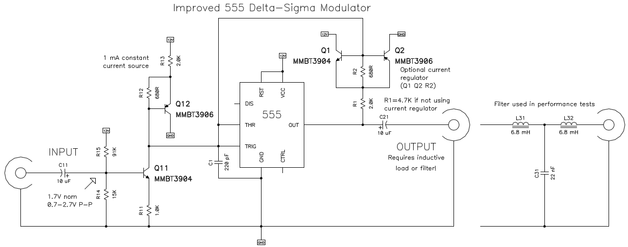
Circuit Notes
- Construction Details
- I built the circuit using the TS555, a fast CMOS version with +/- 100 mA output drive. Most any 555 should work well, although
symmetrical drive (or a good output buffer circuit) and low loading on the threshold and trigger pins is preferred.
- As built and tested, the polarized capacitors are tantalum, the output filter capacitor (C31) is film, and the timing capacitor
(C1) is ceramic. Replacing C1 with a film capacitor may improve performance.
- The input circuit shown is biased for consumer audio line input levels (2V peak-to-peak maximum). Adjust as required if your
needs are different.
- Operating frequency with the values shown is apx. 400 KHz (see measured performance numbers, below).
- To change the operating frequency, modify the timing capacitor value (C1) and/or the current feedback from the output (R1 or
Q1/Q2/R2). If you change the output feedback current, you will likely also want to scale the input current (R11/R12).
- To change the gain of the delta-sigma stage, scale the input current (R11/R12) with relation to the output feedback current.
Note that it is OK to have gains that result in greater than 100% modulation, the output will just stay in the appropriate state
(high or low) until the input signal returns inside the available modulation range, at which point the output will begin toggling
again. WARNING: While the modulator performs as expected in saturation, your output filter may not like this!
- Theory Of Operation
- The forward drop across Q1 and Q2 (current regulating transistors) likely do not match exactly. This is non-critical, and
results in a simple DC offset at the output (ie: it is the same as having a steady-state non-zero input current applied to
C1).
- Set the current source bias resistors (R1, R13) such that the current sources stay in compliance across the full range of C1
voltages (apx 1/3 to 2/3 VCC). Note that if the 555 output is heavily loaded, you may need to reduce R1 to allow for the output not
being driven fully to the rails.
- The input voltage to current converter (Q11) is also inverting the input signal, which coupled with the inverting 555 quantizer
results in a non-inverted output.
- The exact current provided by Q12 and the biasing of Q11 is not critical. Any deviations from ideal will result in a small DC
offset at the output.
- The output modulation frequency varies depending on the input levels, with the frequency decreasing as the output nears the
rails. The output frequency can even extend to DC (with an over-driven input that keeps the output in saturation). Careful design
of the output filter and the overall system (ie: limiting or accounting for the modulation range) is required to achieve optimum
performance over all operating conditions.
- The single-transistor current sources are essentially emitter followers, with a resistor between the base and emitter. This
provides a nearly constant current (Vbe is fairly constant at lower currents, and the changing current across bias resistors R1
& R13 is reduced by the transistors gain). This arrangement is simpler than more traditional two transistor versions, and seems
more appropriate for a 555 project.
- Possible Improvements
- A low-frequency DC-servo feedback loop can keep the operating point centered, if this is important to your application.
- Replacing the input single transistor current sources (Q1, Q2, Q12) with more traditional two transistor versions may improve
performance.
- Replacing the feedback current source (Q1, Q2, R1, R2) with a true voltage to current converter may improve performance. I do
not think this should be necessary unless the output is a very poor approximation of a square wave.
- An output buffer suitable for turning the basic delta-sigma modulator shown here into a window-rattling audio amp, arc-welder,
or other high-powered device is left as an exercise for the reader. :)
See below for real performance data at various operating points.
Performance


- Performance measurements were taken using a Tek AM700 Audio Measurement Set.
- Power was supplied by a PC power supply, with the PC still attached. This is *NOT* recommended for the highest performance (any
noise on the supply will pretty much be directly coupled to the output), but it's what I had handy.
- All performance measurements were taken using the output filter shown in the Improved schematic, above. A more appropriate output
filter would improve performance, particularly at higher frequencies.
- Input and output connections were made by directly tying the differential I/O of the Tek AM700 to the unbalanced I/O of the 555
delta-sigma modulator, which is likely not helping the performance numbers any.
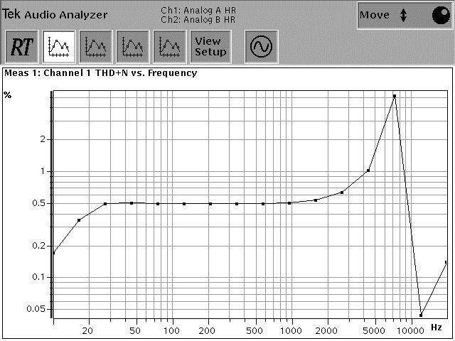
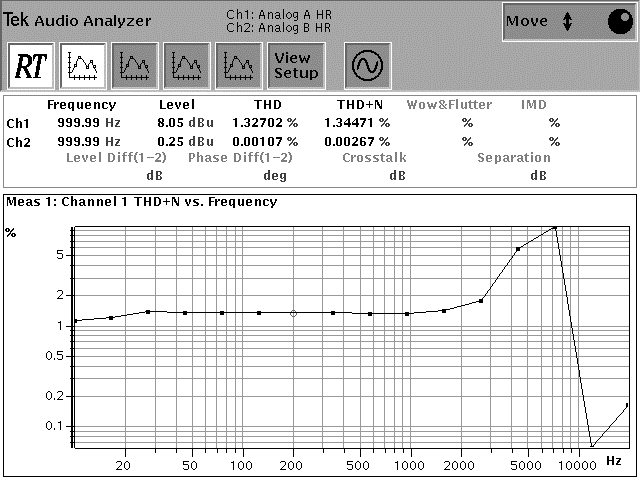
- Performance numbers below were all taken with a 1 KHz sine wave reference. See the images to the right for performance at various
frequencies.
Performance with 1 KHz sine wave
| C1 value |
Test Circuit |
Center Frequency |
Output Level |
Performance |
| Volts P-P |
dBu |
THD % |
THD+N % |
| 220 pF |
Improved |
378 KHz |
|
10 dBu |
|
0.53% |
| Basic |
460 KHz |
|
2.89% |
| 460 KHz |
|
8 dBu |
|
1.41% |
| 330 pF |
Improved |
270 KHz |
|
10 dBu |
|
0.54% |
| Basic |
329 KHz |
|
2.84% |
| 329 KHz |
|
8 dBu |
|
1.34% |
| 470 pF |
Improved |
210 KHz |
|
10 dBu |
|
0.55% |
| Basic |
257 KHz |
|
2.85% |
| 257 KHz |
|
8 dBu |
|
1.37% |
| 680 pF |
Improved |
145 KHz |
|
10 dBu |
|
0.56% |
| Resistor |
178 KHz |
|
2.93% |
| 178 KHz |
|
8 dBu |
|
1.37% |
|
Performance at various output levels
|
| 220 pF |
Improved |
378 KHz |
11 V |
13.4 dBu |
1.47% |
1.51% |
| 10 V |
12.6 dBu |
0.82% |
0.83% |
| 9 V |
12.0 dBu |
0.67% |
0.69% |
| 8 V |
11.1 dBu |
0.55% |
0.56% |
| 7 V |
9.8 dBu |
0.42% |
0.44% |
| 6 V |
8.5 dBu |
0.34% |
0.36% |
| 5 V |
6.8 dBu |
0.27% |
0.32% |
| 4 V |
4.7 dBu |
0.20% |
0.30% |
| 3 V |
2.1 dBu |
0.14% |
0.33% |
| 2 V |
-1.3 dBu |
0.08% |
0.46% |
| 1 V |
-8.5 dBu |
0.05% |
1.03% |
Updates

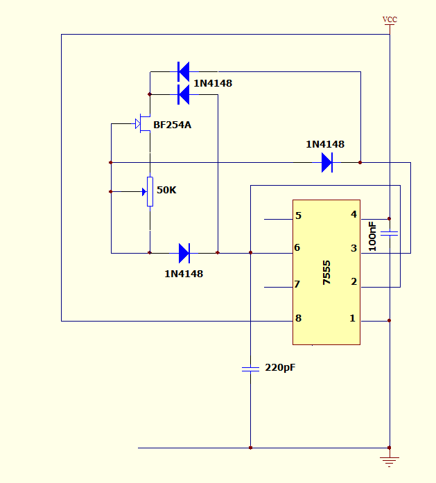
Triangle wave generator with FET
regulated current feedback
Feedback from the 'net: In this design, a FET based current regulator is used for the feedback loop to improve the performance of the
triangle wave generator. This FET circuit could also be used to directly replace the 2-transistor / 2 resistor current regulator in my
improved circuit, above.
